- HOME
- Products
- Basic materials
- Technical conditions
- Technological equipment
- CAD CAM
- The Laser Photoplotter
- CNC drilling and routing
- UV Laser drilling and routing
- Laser Tannlin TX PROi
- Direct plating
- Vyplňování otvorů | Planarizer
- Surface readjustments
- Surface finishes
- Galvanic processes
- Digital Direct Imaging
- The etching
- Solder mask and silkscreen
- Inspections of PCB
- Controlled impedance
- Multilayer lamination
- Contour fabrication
- Analytical Laboratory
- PCB Designs
- PCB assembly
- Terms and Conditions
- Preislist
- Contact
- kariéra
Design and base construction
Our company offers almost the entire range of rigid PCBs. We offer a wide range of basic laminate thickness and copper foil, different colors of solder mask and serviceprint, several surface of finishes. Everything can be more or less arbitrary. If you do not have special requirements for the product or give the exact technical specifications, it is understood this basic form:
- base material VENTEC VT-47 1,55mm
- base Cu 18µm ( + plating ca 25µm )
- green soldermask
- white positionprint
- H.A.S.L. surface ( or in the case of fine SMD chemical golding )
- routing
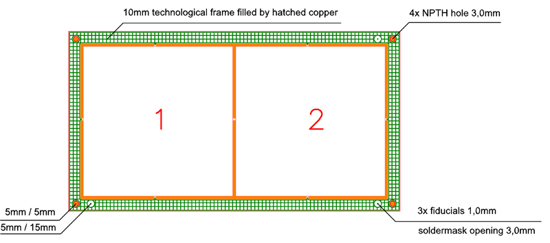
If a panelization is requested and the frame is not precisely specified by the customer, it will be made according to the design in the figure. The size of the frame is including the milling or grooving tool. A process frame below 7mm for a milled panel is mechanically unsuitable.
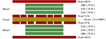
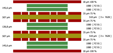
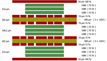
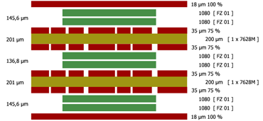
base stack-up of multilayer:
|
|
2-sided PCB´s, thickness 1,5mm, final Cu foil thickness 35µm |
| 4-layer PCB´s, thickness 1,5mm, final Cu foil thickness 35µm |
|
|
|
4-layer PCB´s, thickness 1,5mm, final Cu foil thickness 70µm |
| 4-layer PCB´s, thickness 1,0mm, final Cu foil thickness 35µm |
|
|
|
6-layer PCB´s, thickness 1,5mm, final Cu foil thickness 35µm |
| 6-layer PCB´s, thickness 1,5mm, final Cu foil thickness 70µm |
|
|
|
6-layer PCB´s, thickness 1,0mm, final Cu foil thickness 35µm |



 company adress :
 place of business :


