- HOME
- Products
- Basic materials
- Technical conditions
- Technological equipment
- CAD CAM
- The Laser Photoplotter
- CNC drilling and routing
- UV Laser drilling and routing
- Laser Tannlin TX PROi
- Direct plating
- Vyplňování otvorů | Planarizer
- Surface readjustments
- Surface finishes
- Galvanic processes
- Digital Direct Imaging
- The etching
- Solder mask and silkscreen
- Inspections of PCB
- Controlled impedance
- Multilayer lamination
- Contour fabrication
- Analytical Laboratory
- PCB Designs
- PCB assembly
- Terms and Conditions
- Preislist
- Contact
- kariéra
Peelable mask
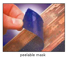
The peelable mask is applied by screen printing and it is a mask intended for protection of specific areas of the printed circuit boards during the metallizing procedures. It was designed to protect against soldering processes and it is resistant to wave soldering and tinning by H.A.L technologies. It forms a temporary coating, easily removable by hand without leaving any trace in metallized holes or on the board’s surface.
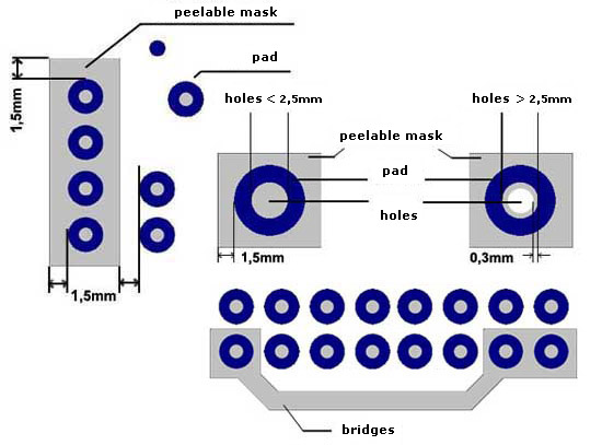
 the surface covered by a peelable mask has to be minimally 1,5mm larger than the covered area and the distance from the nearest uncovered spots has to be larger than 1,5mm. the surface covered by a peelable mask has to be minimally 1,5mm larger than the covered area and the distance from the nearest uncovered spots has to be larger than 1,5mm. masking of the holes < 2.5mm is without problem. To prevent penetration of varnish through a drilled hole > 2,5mm during the masking, it is necessary that the peelable mask overlaps the edge of the drilled hole by about 0,3mm. masking of the holes < 2.5mm is without problem. To prevent penetration of varnish through a drilled hole > 2,5mm during the masking, it is necessary that the peelable mask overlaps the edge of the drilled hole by about 0,3mm. you remove the mask from individual areas of printed circuits more easily if you use a connecting bridge. you remove the mask from individual areas of printed circuits more easily if you use a connecting bridge.
|
|


 company adress :
 place of business :


