- HOME
- Products
- Basic materials
- Technical conditions
- Technological equipment
- CAD CAM
- The Laser Photoplotter
- CNC drilling and routing
- UV Laser drilling and routing
- Laser Tannlin TX PROi
- Direct plating
- Vyplňování otvorů | Planarizer
- Surface readjustments
- Surface finishes
- Galvanic processes
- Digital Direct Imaging
- The etching
- Solder mask and silkscreen
- Inspections of PCB
- Controlled impedance
- Multilayer lamination
- Contour fabrication
- Analytical Laboratory
- PCB Designs
- PCB assembly
- Terms and Conditions
- Preislist
- Contact
- kariéra
SemiFlex
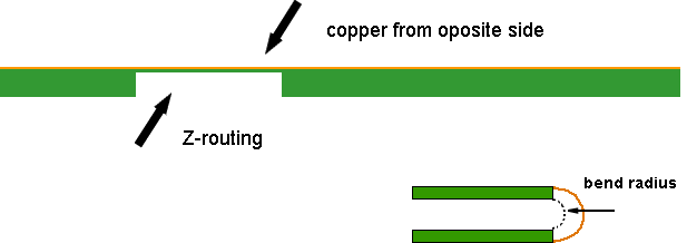
Semiflex printed circuit boards are a variant for those for whom the production of FLEX-RIGID circuit boards is expensive and uneconomical. They are the solution for applications where the flexible part does not move during operation, where space is needed and where neat product design is required. The production is very similar to the production of standard rigid printed circuit boards, except that at the end of mechanical treatment, part of the board is Z-routed to the required depth.

The depth and size of the Z-routing surface is given by the PCB design and technical description. This area in the mechanical layer must be clearly specified in the data. It is recommended to fill the other side of the flexible part with a copper surface. There should be no drilled holes or cutouts in this area. The drilled holes should be at least 1mm away from the edge of the flexible / rigid part. The rest of the material after Z-routing should be in the range of 0.15 - 0.25mm. It is recommended to use a flexible solder mask on the PCB.
| Bend radius | requested length of the Z-routing area |
| 45° | 5 mm |
| 90° | 10 mm |
| 180° | 20 mm |


 company adress :
 place of business :


