Copper balance on a printed circuit board is very important because unbalanced copper can cause PCB defects and errors, such as twisting, delamination, or poor electroplating of a conductive pattern that the manufacturer cannot influence.
1/ PCB twist :
- If there are unsymmetrical copper surfaces on the PCB, it can be distorted by thermal processes such as lamination, hot air leveling, or subsequent soldering wave. Correct, symmetrical distribution of conductors and copper surfaces eliminates twisting error.
2/ PCB delamination :
- The problem arises mainly from the use of thicker copper (50um or more) on cores on which the copper surface is unbalanced. Worse, where there are motifs with little copper filling. In this case, the copper surfaces need to be supplemented with a "false" area or flats to prevent overflowing of the prepreg into the motifs and subsequent delamination or interlayer short-circuit.
|
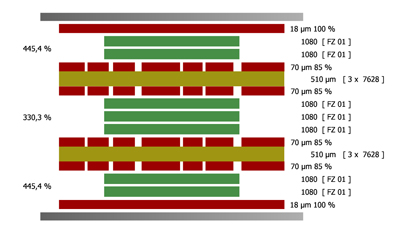
YES
85% of copper is filled in the inner layers, so filling the prepregs is sufficient and there is no risk of delamination
|
NO
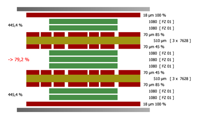
copper is only 45% filled in the inner layers, so filling the prepregs between layers is insufficient and there is a risk of delamination
|
3/ Poor electroplating of the conductive pattern :
- For the correct setting of the galvanic process, the copper balance on the conductive layers is very important. If copper is unbalanced at the top and bottom, or even at each individual layer, overplating can occur, and lead to connected tracks or underetching. In particular, this relates to differential pairs with measured impedance values. Setting the correct galvanic process is complicated and sometimes impossible. It is therefore important to replenish the copper balance with "false" patches or full copper.
|
YES
|
NO
|


 company adress :
 place of business :